Processing-in-Memory for Decode-Stage GEMV: Mixed-Signal, Digital, and the Cost of Noise
A tour of decode-stage GEMV acceleration via processing-in-memory: memory cell types, mixed-signal vs. digital PIM designs, and the accuracy cost each trades for throughput.
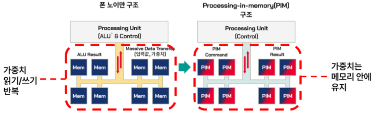
Von Neumann accelerators (by-bus) architecture hit the memory wall. PIM acceleration is heavily investigated to address this. This post explores PIM-based DNN accelerators: (1) volatile and non-volatile memory cells commonly used for PIM; (2) categories of PIM accelerators (digital vs. mixed-signal/analog processing); (3) operational accuracy.
01. Background
A. Hardware Architecture
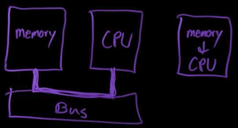
In a traditional von Neumann architecture, a computer has two main blocks — memory and CPU — connected by a bus. Every operation requires shuttling data back and forth across that bus.
Instead of passing whole data by bus, in-memory computing performs computation directly where data is stored (inside or very near the memory array). PIM (Processing-in-Memory) is the hardware approach that implements this — embedding compute logic inside the memory chip itself (e.g., inside DRAM banks).
B. Linear Algebra in Machine Learning Workload
BLAS (Basic Linear Algebra Subprograms) is a standard set of low-level routines for performing common linear algebra operations. Chip vendors have built their own BLAS libraries optimized for their hardware — like NVIDIA’s cuBLAS and Intel’s oneAPI Math Kernel Library (oneMKL).
BLAS consists of 3 levels:
- vector-vector operations (e.g., dot product); $y \leftarrow ax + y$
- matrix-vector operations (GEMV); $y \leftarrow \alpha Ax + By$
- matrix-matrix operations (GEMM); $y \leftarrow \alpha AB + \beta C$
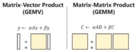
In the prefill stage, GEMM is the biggest bottleneck because multiple tokens’ activations are stacked into a matrix and multiplied against weights all at once.
Unlike the prefill stage, GEMV is the biggest bottleneck in the decoding stage, because the weight matrix and activation vector (hidden state) must be loaded and computed iteratively.
C. Memory Technologies
a. Volatile Memories (VM)
VM is memory that loses its data when power is turned off. DRAM (Dynamic RAM) and SRAM (Static RAM) are both VM, but differ in structure and use:
- DRAM: Stores each bit using a capacitor + transistor. It’s denser and cheaper, but the capacitor leaks charge over time, so it needs to be “refreshed” (re-written; dynamic).
- SRAM: Stores each bit using a set of transistors (usually 6) in a flip-flop circuit, with no need for refreshing (no capacitor). It’s faster and more power-efficient per access (since it doesn’t require refresh), but much more expensive.
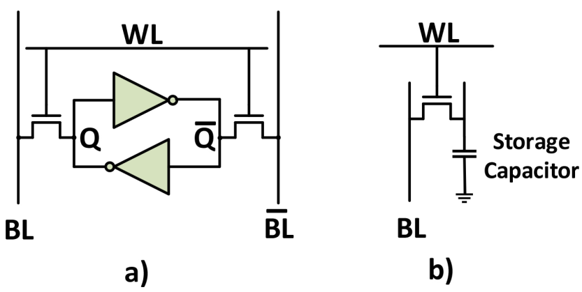
Compared to NVM (not-VM), SRAM offers lower read latency but suffers from increased leakage power at high temperatures. SRAM cells are often used in PIM architectures to perform MAC operations due to their speed, rather than as main memory (which is typically DRAM’s role).
At the moment, DRAM is the most popular type of memory, favored for its simple design and low cost. DRAM’s capacitance leaks current and data has to be transferred to the main chip, so high latency and power are needed. There are new techniques to challenge this, but DRAM’s biggest concern still seems to be its scaling limit with newer technologies and smaller transistor sizes.
b. Non-Volatile Memories (NVM)
To address the aforementioned disadvantages of VM, NVM emerges. It has the ability to retain data even if the power supply is disconnected. Some of the most popular NVM types are flash memory, resistive random-access memory (ReRAM or RRAM), and ferroelectric RAM (FeRAM, F-RAM, or FRAM).
A flash memory cell is simply a MOSFET cell. A ReRAM cell consists of one memristor and one transistor. A memristor is a device that acts as a programmable resistance, so the voltage level across the transistor can be determined.
This post doesn’t deep-dive into hardware like MOSFET
02. Why In-Memory Computing Helps Decode-Stage GEMV
As in-memory architectures’ main idea is to perform the target operations inside memory, there are two main trends: mixed-signal-based and digital-based.
A. Mixed Signal Approach
Computation uses the analog properties of the memory cell. A DAC converts the digital input into a voltage, applied to the memory cell storing the weight (as conductance). Each cell turns that voltage into a current, and the bitline sums the currents by Kirchhoff’s current law — the MAC happens as physical charge accumulation, not ALU ops. An ADC converts the summed result back to digital.
Since the weight matrix is already resident in the crossbar, a decode-stage GEMV runs as a single analog pass instead of repeatedly streaming weights across a bus — throughput matches GEMV’s MAC-dominant access pattern directly.
B. Digital Approach
Computation is done completely digitally — no DAC/ADC required. Weights and activations are decomposed or quantized (e.g., to binary), turning MAC operations into bit-wise logical operations (AND, OR, etc.) followed by additions and shifts, which the memory cells and supporting digital blocks perform.
The trade-off between the two is clear. Mixed signal is faster for MAC operations, but ADC/DAC eat up a lot of chip area and power. Digital avoids that overhead and is more power-efficient, but decomposing ops into bits adds latency, and low-bit quantization limits which neural networks it can handle accurately.
03. The Cost of Moving Compute Into Analog: Noise
That throughput isn’t free — it’s paid for in DACs/ADCs, which can eat up to 23% of chip area and 61% of power, or in extreme cases up to 99% area and 85% power.
Mitigations: eliminate the DAC and serialize the activation bit-by-bit (shrinks the ADC too, but costs more cycles — roughly one per bit of activation precision), or bit-decompose the weight as well, trading cycle count against converter size.
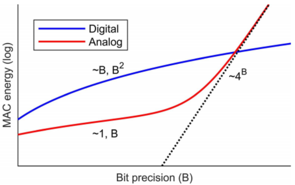
At low bit precision, analog MAC energy stays roughly flat (~1, ~B) — well below digital’s ~B, B² growth. But it scales as ~4^B at higher precision and crosses above digital. So the crossbar only wins in a narrow low-precision band, which is exactly where conductance noise and limited ADC resolution bite hardest — analog compute doesn’t just risk noise, it requires operating where noise is hardest to hide.
None of this explains how a network becomes noise-robust, though. IBM’s PCM work does: during training, inject a random noise term into the weights on the forward pass — sized to the real device’s read/write noise — then backprop and update as normal. The network learns to tolerate its target hardware’s actual noise distribution, not just lower precision. That’s distinct from fixed-point quantization, where rounding error is deterministic, so training against rounding alone doesn’t confer robustness to random conductance drift or device-to-device variability.
04. Data Representations for Quantization
Fundamentally, quantization swings within trade-off: the less representation space it have, the more memory footprint reduction derived, with the more accuracy loss. There are variable target representations, each a different point on the throughput/power/accuracy:
- Floating point (FP): most accurate, used for training, widest network support — but needs expensive high-throughput power blocks.
- Fixed-point (INT; Integer): most popular for IMC today; weights as low as 4-bit boosts throughput
- Binarized: Single bit per cell, MAC becomes a simple logical op; accuracy loss can be recovered by binarization techniques.
- Mixed precision: spans binarized to full FP in one architecture via the same bit-decomposition/serialization tricks from §03, trading precision for throughput/power dynamically — at the cost of extra control hardware (e.g., a hierarchical network-on-chip).
- MXFP / NVFP (2025-era, digital accelerators): block floating-point which shares exponent per block of values, individual mantissas per element — is how NVIDIA Blackwell and the OCP microscaling spec now solve the same problem.
In the next post: a deep-dive into Sparse Attention in hardware, and CapRAM (a proprietary analog in-memory compute (CIM) architecture developed by SEMRON).
References
- (SK HYNIX newsletter) 메모리 기반 연산 가속기: 저장과 연산을 동시에 하는 진정한 두뇌로: https://news.skhynix.co.kr/dgist-series-1/
- (Fraunhofer IPMS / Bosch, 2022) Laleni, Soliman, Vardar, Kämpfe. “Emerging In-memory Computing for Neural Networks”: https://www.ipms.fraunhofer.de/content/dam/ipms/common/documents/2022/Fraunhofer%20IPMS-Bosch-Emerging%20In-memory%20Computing-for%20Neural-Networks.pdf
- (IBM youtube) What is In-Memory Computing?: https://youtu.be/BTnr8z-ePR4
- “Tutorial: Analog Matrix Computing with Crosspoint Resistive Memory Arrays”: https://arxiv.org/pdf/2205.05853